
Equipment principle:
Use two high-precision cameras up and down to move the same board
According to the image, the convolutional neural network algorithm is adopted to process the image, and the intelligent judgment unit
Bad parts and bad soldering.
Suitable products:
High standard category: automotive electronics, military industry, aerospace;
Motherboard category: server motherboard, PC motherboard;
Netcom category: communication board, Netcom board;
Control category: industrial control board, smart home appliance board;
Electric meter category: dashboard;

插件不良

Bad patch

Poor solder
Installation position: before final inspection and packaging
Save personnel and can replace the visual inspection station before final inspection;
Improve quality, effective card control before packaging, poor interception, and avoid outflow;
Data traceability, the photos of the front and back panel cards before packaging can be kept, and the data can be traced;
Visual inspection of front and back before implementation

Installation position: behind smt bilateral craft furnace

After the two-sided process reflow oven: detect both front and back side patch and poor solder paste printing at one time, saving space
1. Deep learning algorithm, simple programming, high detection rate;
2. Achieve one-key programming, automatic search of component solder joints, and fast programming;
3. General intelligent model, training based on big data;
4. Path planning reduces the number of FOV shots and shortens the shooting path;
5. Diversified models, supporting remote plate making, mixed plate production, and online testing;
6. One-click data export, comprehensive and detailed statistical reports, data docking with MES system;
7. Facing Industry 4.0, centralized management reduces personnel;
8. Practical training tools, self-learning and evolution of equipment;
Product Feature 1: Core Algorithm Innovation
Convolutional neural network algorithm is used to solve the two traditional algorithm pain points: long programming time and high false alarms
Intelligent algorithm: Based on deep learning of big data, one-click search for component solder joints, automatic programming, intelligent identification of defective component solder joints
Traditional algorithms: color, edge, feature and other detection and comparison algorithms, etc. OCR text recognition algorithm

Product feature two: easy to learn and operate
Deep learning algorithm, simple programming, one-click automatic search of component solder joints, intelligent judgment of poor, fast programming speed.
Intelligent adjustment algorithm: CAD, Gerber, etc. files are not required, and the solder points and chip materials can be automatically selected and parameters can be set
Parameter broadcast function: One-key synchronization of similar solder joint algorithms and parameters, greatly reducing adjustment time
Online programming: can realize "measure while adjusting", no need to stop the line;
Programming time: 10-20min; debugging time: 10-15min
Short line change time, direct call to existing format files, no need to repeat adjustments

Product feature three: strong detection ability
The model based on big data training has high recognition accuracy of components, strong detection ability and generalization, and can correct alarms caused by diversified solder joint deviations and reduce false alarms.
On the BOTTOM surface under the wave soldering process, the solder joint components vary greatly, and the algorithm is required to recognize different NG and different OK, and cannot miss the test
Convolutional neural network is more similar to the way of human discrimination. It can effectively identify diverse test scenarios and reduce the false alarm rate while ensuring the detection rate.
Strong ability to identify fuzzy features and effectively detect tin holes on solder without interference from pins and devices
Strong generalization ability, compatible with multiple shapes of solder joints, diversified solder joints, slight differences in color, irregular solder joints, and low false alarm rate
Product feature four: fast detection speed
Genetic algorithm path planning
Fewer FOVs-the positions without solder joints are not shot, reducing the number of FOVs and improving efficiency;
Shorter photo path-reduce FOV jumps with a large span, further saving time;
More suitable imaging position-avoid soldering points at the FOV connection to ensure test results;
GPU image parallel processing, data running faster;

Product feature five: multiple detection modes
Combining with the diversification of factory production modes, design a variety of testing modes to support testing of multi-model production and alternative materials;
Support puzzle detection Support mixed board detection BadMark skip mode

Product feature six: detailed test data
Test data is retained in real time, and detailed data reports can be exported, which is conducive to process improvement and production traceability;
The camera automatically reads the barcode (barcode, dot code);
Data integrity: including overall statistical data, and all inspection information of each inspection board;
One-click export: easy to trace back, data can be effectively connected with the MES system

Product feature seven: centralized management, remote service
Support remote programming, debugging, management, save time for changing lines, and support one-to-many re-judgment
Remote debugging, control and centralized management: reduce work interruption and improve work efficiency
Remote offline programming, advance programming
Remote support: quick response to maintenance
Re-judgment workstation: one-to-many re-judgment

Product feature eight: wide detection range
AI tool training model, equipment end can independently train special devices, can automatically identify, improve detection accuracy
Quickly learn new devices and solder joints
Debug the program, adjust the threshold to treat the symptoms but not the root cause. Through training, let the equipment recognize the different forms of the device, and truly reduce the false alarm rate
Rapid iteration and continuous upgrading of testing capabilities

Product feature nine: equipment details
Three-section adjustable width track design: save the time of entering and exiting the board and improve the detection efficiency
Stainless steel roller conveyor belt: wear-resistant, strong load, easy to maintain
Automatic cleaning device of detection module: Automatically clean the surface dust to avoid detection interference. Working height can be selected according to the height of the production line

Projection rework station (online/offline)
Avoid manual searching, improve maintenance efficiency, and avoid omissions;
Support single point/multipoint mark bad point mode;
Single point/multipoint projection, high alignment accuracy;
Support multi-station operation and improve maintenance efficiency
A variety of guide color options to avoid color interference on the layout
Guide maintenance in different areas, more efficient;
Flat/inclined maintenance track, can be customized according to customer's situation;

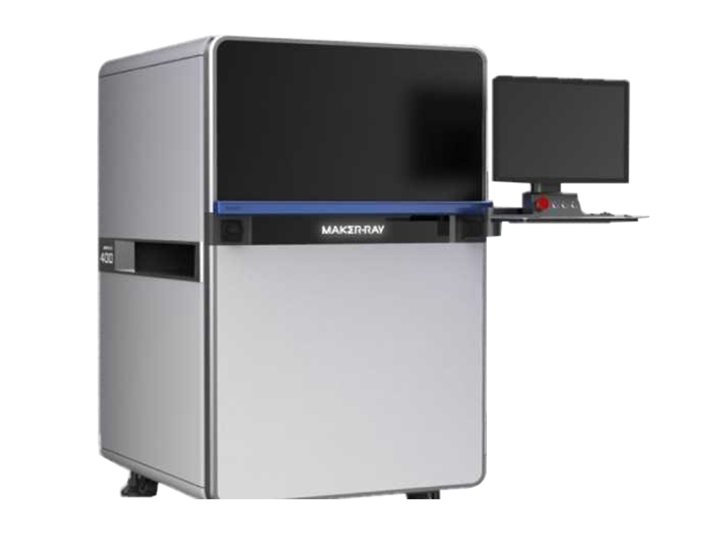
类别 | 项目 | 在线PCBA双面光学检测设备AIS501 |
PCBA规格 | 尺寸 | 50x50mm~510*460mm |
厚度 | 0.5mm-6mm | |
元件高度 | 顶面:50mm,底面:50mm | |
工艺边 | 3mm | |
光学规格 | 相机 | 上相机:5MP彩色面阵高速工业相机 上相机:5MP彩色面阵高速工业相机 |
光源 | RGB+W四色积分光源 | |
FOV | 20um@45*37mm;15um@36*30mm | |
分辨率 | 20以m 或15um | |
检测相关 | 元件检测 | 手插元器件及贴片料的缺件、反转、偏移、破损、歪斜、多插、异物、污损等 |
焊锡检测 | 多锡、少锡、连锡、不出脚、空焊、虚焊/锡洞等 | |
其他功能 | 一维/二维码识别/字符识别等 | |
混板测试 | 混板生产,支持程序自动调用 | |
算法 | 深度神经网络算法,图像对比,颜色对比,轮廓识别,偏移检测,模板匹配,OCR等 | |
速度 | 0.23sec/FOV |
类别 | 项目 | 在线PCBA双面光学检测设备AIS500 |
软件系统 | 操作系统 | Ubuntu 18.04 LTD 64bit |
功能 | 远程控制、远程协助、gerber文件导入、自定义模型训练 | |
通讯方式 | 标准S MEMA接口 | |
数据输出 | 自动生成统计分析SPC | |
特色功能 | 元件自动搜索、一键编程 | |
硬件规格 | 工控主机 | CPU: intel i7 显卡:Nvida独立GPU加速卡 存储:64G DDR,256G SSD+2T机械硬盘 网络:1000M有线网卡 |
显示器 | 22寸 FHD显示器 | |
运动机构 | 高精度丝杆+伺服电机 | |
轨道调宽 | 手动/自动 | |
外观/电气 | 机箱尺寸及重量 | 1050x1335x1650mm, 1000Kg |
电源及功率 | AC 220V,额定功率4000W | |
气源 | >0.5Mpa | |
工作环境 | 温度:10~45°C,湿度:30~85%RH |


 中文
中文 English